Printing and Fabrication Applications
Nanoscribe - 3D Lithography system
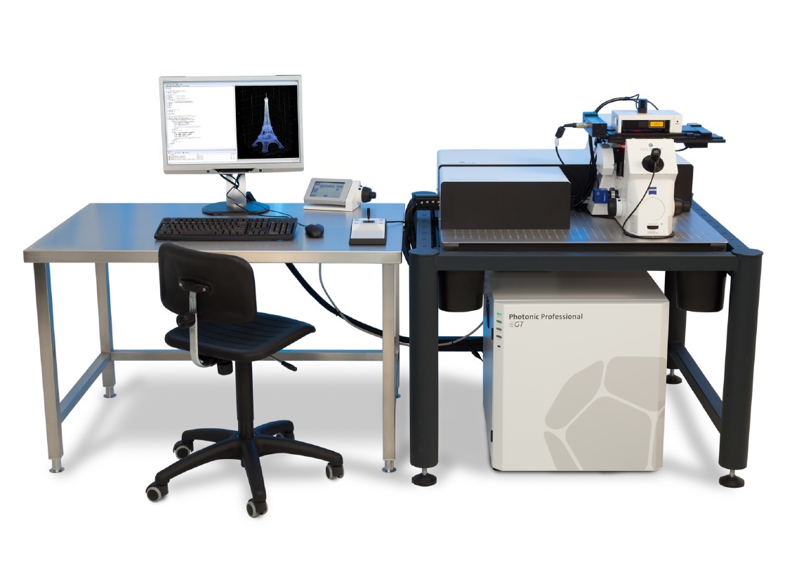
Useful for:
- Useful for fabricating high precision devices e.g. microlenses
- Non-clogging micro-porous SU-8 filters
- Targeted drug delivery systems
- Fabrication of cell scaffolding to promote cell adhesion
- Manufacturing fractal-like architectures to attain various mechanical properties
- Allows for printing of arrays

100 micron Icosahedron Printed on Nanoscribe Photonics GT
Micro Fab - Jetlab II Inkjet Printer
Useful for:
- Life-Science related research: Useful for studying behavior for Antibodies, Proteins, Nucleic acids, and Viruses
- Inorganic Research: Adhesives, Colloidal particles, Quantum dots, Etchants, and Solvents
Exaddon Ceres Metal 3D Printer

The Exaddon Ceres Metal 3D Printer prints microscale objects using electrodeposition. With a printable size range of 1 μm – 1 mm with < 1 μm resolution, this tool is optimal for applications in brain-machine interfaces, semiconductor surface modification, Photonics, Drug Delivery and HF communication components.
Tool Specifics:
- Prints with pure metals such as nickel, copper and gold.
- Prints at room temperature with no post-processing necessary
- Optimized for printing free-standing microscale structures such as pillars, needles, coils, and lattices on existing surfaces, such as ICs or wafers
BMF MicroArch S-140

The BMF MicroArch S-140 is the ideal solution for researchers requiring ultra-high resolution, accuracy, and precision in a desktop micro 3D printer. The BMF microArch is the first commercialized high-resolution, 3D microfabrication equipment based on PμSL technology. Projection Micro Stereolithography allows for rapid photopolymerization of a layer of liquid polyer using a flash of UV-LED at micro-scale resolution. Experience the fast and easy production of microstructures by importing your STL file and exposing your design directly to accelerate your work in the areas of microfluidics, MEMS, filtration, electronics, medical devices, and other applications that require microstructures.
Tool Specifics:
- Large build volume 94x52x45mm
- Optical resolution of 10μm and layer thickness of 10-40μm
- Can produce surface finishes of 0.4 - 0.8μm Ra (top) and 1.5 - 2.5μm Ra (side)